
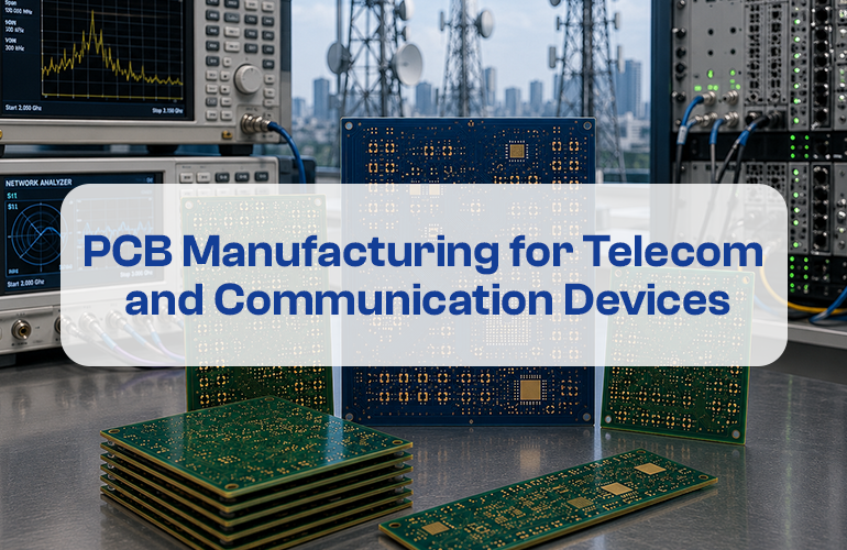
PCB manufacturing for telecom and communication devices requires high precision, signal stability, and reliable performance. Communication systems depend on accurate data transmission, and even small PCB issues can affect speed, signal quality, and overall system performance.
Telecom PCBs are used in networking equipment, RF modules, antenna systems, routers, base stations, communication controllers, and high-speed electronic devices.
Therefore, manufacturers must build these PCBs with proper material selection, impedance control, and advanced testing to ensure consistent performance.
Why Telecom PCBs Are Different
Telecom and communication devices often handle high-speed and high-frequency signals. These signals are sensitive to several PCB design factors, including:
- Material selection
- Trace geometry
- Impedance control
- Layer arrangement
- Signal spacing
Because of this, standard PCB manufacturing methods may not always meet telecom requirements. Instead, manufacturers need controlled processes that focus on signal integrity and reliability.
Material Selection for Telecom PCBs
Material selection plays an important role in telecom PCB manufacturing. The right material helps maintain stable electrical performance, especially in high-frequency applications.
FR4 works well for many standard communication boards. However, advanced RF and high-frequency applications may require materials such as Rogers, PTFE, or other specialized materials.
Additionally, selecting the correct material helps reduce signal loss and improves long-term PCB performance.
Controlled Impedance for Signal Stability
Controlled impedance is essential for high-speed communication signals. If impedance values change during manufacturing, signals can experience reflection, distortion, or reduced strength.
Engineers consider factors such as:
- Trace width
- Copper thickness
- Dielectric thickness
- Layer stack-up
Therefore, proper impedance planning helps maintain accurate signal transmission in telecom applications.
Multilayer PCB Support
Telecom devices often require compact designs with complex routing requirements. Multilayer PCBs help engineers manage:
- Signal routing
- Power distribution
- Ground planes
- Shielding requirements
Moreover, proper stack-up planning and layer alignment improve signal stability and manufacturing consistency.
Fine Track and Spacing Requirements
Communication devices continue to become smaller and more powerful. As a result, PCB designs require higher circuit density and precise routing.
Fine track PCB manufacturing helps engineers fit more connections into limited board space.
Accurate track width and spacing are important because they affect both manufacturing quality and signal performance.
Testing and Inspection
Testing is a critical step in telecom PCB manufacturing. Before assembly, manufacturers inspect boards to confirm quality and reliability.
Common testing methods include:
- AOI inspection
- Flying probe testing
- Impedance testing
- Electrical inspection
These tests help identify connectivity issues, signal problems, and manufacturing defects before the PCB reaches the final application.
How True PCB Supports Telecom and Communication PCBs
True PCB supports telecom and communication PCB requirements through advanced manufacturing capabilities, including:
- Multilayer PCB fabrication
- Controlled impedance boards
- Fine track designs
- Special material support
- Precision manufacturing processes
These capabilities help engineers develop communication boards that require stable signal performance, compact designs, and reliable operation.
Additionally, True PCB supports testing and inspection requirements to ensure that telecom PCBs meet application-specific performance expectations.
Conclusion
PCB manufacturing for telecom and communication devices requires careful control over signal integrity, material selection, impedance, and layer structure.
Every design and manufacturing detail affects communication performance. By choosing the right manufacturing approach, companies can develop reliable PCBs for networking, RF, and high-speed communication applications.