
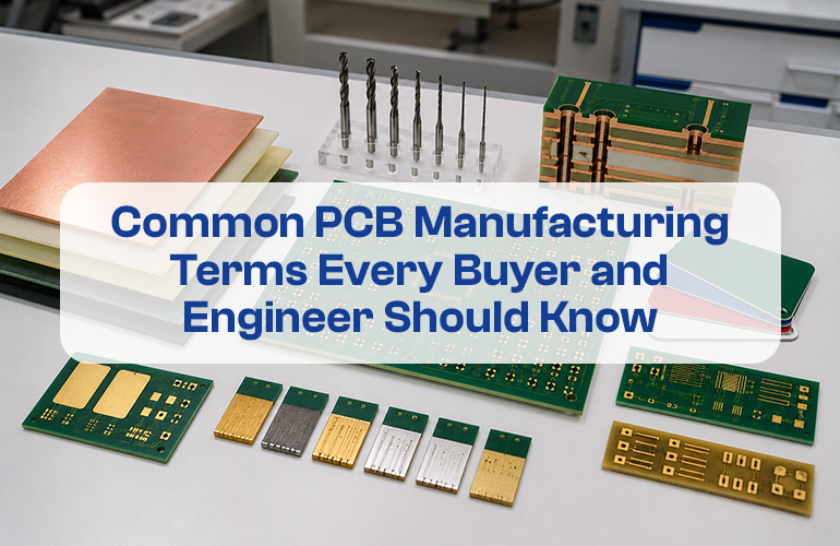
Understanding PCB manufacturing terms is crucial for buyers, engineers, and product teams. These terms help improve communication with manufacturers, reduce errors, and ensure smoother production. Whether ordering prototype PCBs or planning small batch production, knowing key terms improves accuracy and efficiency.
PCB Prototype
A PCB prototype is an early version of a printed circuit board used for testing and validation. It helps engineers check design performance before moving to larger production. Prototypes are essential for identifying design errors, improving functionality, and reducing production risks.
Gerber Files
Gerber files are the standard production files used in PCB manufacturing. They detail copper layers, solder mask, silkscreen, paste layers, and board outline. Accurate Gerber files are essential for the manufacturer to produce the PCB correctly.
Drill File
A drill file specifies holes, vias, and slots on the PCB. It shows exact hole locations, sizes, and whether they are plated or non-plated. Correct drill files prevent assembly issues and ensure reliable electrical connections.
Copper Thickness
Copper thickness impacts current carrying capacity, heat management, and overall circuit performance. High-current applications and power electronics often require thicker copper for optimal reliability.
Solder Mask
The solder mask is a protective layer over copper tracks. It prevents solder bridges, protects the copper, and enhances PCB durability. While green is common, other colors are available depending on manufacturing requirements.
Silkscreen
Silkscreen refers to printed text or markings on the PCB, which identify components, polarity, test points, and other critical information. Clear silkscreen ensures easier assembly, maintenance, and inspection.
Surface Finish
A surface finish protects exposed copper and improves solderability. Common finishes include HASL, ENIG, immersion tin, immersion silver, and OSP. The right surface finish depends on assembly, shelf life, and application requirements.
Multilayer PCB
A multilayer PCB contains more than two conductive layers. These boards provide more routing space for compact and high-performance electronics. Proper stack-up planning and manufacturing control are critical for multilayer designs.
Flying Probe Testing
Flying probe testing is an electrical testing method that checks PCB connectivity without a dedicated fixture. It is ideal for prototypes and small batch PCBs, detecting open circuits, short circuits, and connectivity issues early.
How TruePCB Supports Better PCB Manufacturing Understanding
TruePCB works with engineers, startups, and product teams across prototype and small batch PCB manufacturing. Their support includes:
- Guidance on PCB types and material selection
- Assistance with Gerber file preparation, drill files, and stack-up planning
- Testing support including AOI, flying probe, impedance, and contamination testing
- Expert advice for surface finish, copper thickness, and special requirements
This ensures customers make informed decisions, reduce production risks, and communicate clearly with the manufacturing team.
Conclusion
Understanding common PCB manufacturing terms—including Gerber files, drill files, solder mask, copper thickness, surface finish, multilayer PCB, and flying probe testing—is essential for accurate production. Clear technical knowledge helps engineers and buyers avoid delays, prevent errors, and improve the quality of the final PCB. Partnering with True PCB provides additional guidance, ensuring reliable prototypes and small batch boards ready for production.