
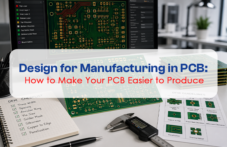
Design for Manufacturing in PCB, also known as PCB DFM, helps engineers create designs that are easier, faster, and more reliable to manufacture. A PCB may work well in design software, but it still needs to be practical for real production.
When DFM is considered early, it reduces production delays, lowers the chances of errors, and improves PCB quality. For prototype and small batch PCB manufacturing, DFM becomes even more important because every design version should move smoothly into production.
What Is PCB Design for Manufacturing?
PCB Design for Manufacturing means designing the board in a way that matches the manufacturer’s production capabilities. It includes track width, spacing, hole size, copper thickness, solder mask clearance, surface finish, stack-up, and material selection.
The goal is simple. The PCB should not only function electrically but also be manufacturable with consistency.
Why DFM Matters
Poor DFM can create manufacturing challenges. These may include broken tracks, insufficient spacing, drill issues, solder mask problems, copper imbalance, or assembly difficulty.
When the PCB is designed with manufacturing in mind, these problems can be reduced before production begins. This saves time and improves output quality.
Track Width and Spacing
Track width and spacing should match the manufacturer’s capability. Very narrow tracks or spacing may need advanced production control.
If the track width is too small for the selected copper thickness, the design may become difficult to manufacture. Engineers should check these values before submitting files.
Drill Size and Hole Quality
Drill holes are used for vias, component leads, slots, and mounting points. Incorrect drill sizes can create assembly and connectivity issues.
A DFM-ready PCB should include clear drill files, correct hole sizes, and proper plated or non-plated hole information.
Solder Mask and Silkscreen
Solder mask helps protect copper and prevent solder bridges. Silkscreen helps identify components and assembly details.
If solder mask openings are too small or silkscreen overlaps exposed pads, assembly problems may occur. These small details should be checked during DFM review.
Material and Surface Finish Selection
Material and surface finish should match the board’s application. High-frequency boards, power electronics, and thermal applications may need specific materials and finishes.
Choosing these details early helps prevent production confusion and delays.
How True PCB Supports PCB DFM
True PCB supports customers with prototype and small batch PCB manufacturing that benefits from clear design and manufacturing readiness. By working with defined technical specifications, material options, surface finish choices, drilling capabilities, and testing processes, True PCB helps engineers move from design files to production with better accuracy.
For customers developing complex boards, True PCB’s manufacturing support helps identify important production factors such as copper thickness, layer structure, track spacing, and testing needs before the board moves ahead.
Conclusion
Design for Manufacturing in PCB helps reduce errors, improve production quality, and make the board easier to manufacture. It connects design intent with real production capability.
By focusing on DFM early, engineers can save time, avoid repeated corrections, and build PCBs that are ready for reliable testing and application.