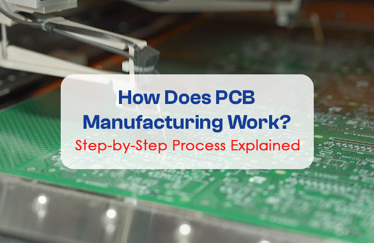
Printed Circuit Boards (PCBs) form the foundation of modern electronic devices. They provide mechanical support and create reliable electrical connections between components. Therefore, understanding the PCB manufacturing process helps designers, engineers, and manufacturers produce high-quality boards. This guide explains each production stage and highlights the machines that improve accuracy and reliability.
Step 1: Designing the PCB Layout
The PCB manufacturing process begins with layout design. Engineers use specialized software to define component placement, routing paths, and layer structures. Next, they export the design in Gerber file format, which serves as the production blueprint.
Step 2: Printing the PCB Design on the Copper Board
Manufacturers transfer the PCB design onto a copper-clad substrate using photoresist technology. They expose the board to UV light to harden specific areas of the photoresist. Afterward, they remove the unexposed sections and prepare the board for etching.
Machine Example:
Inkjet Printer for Legend Printing – Prints high-resolution text, symbols, and identification marks quickly and accurately. As a result, assembly teams can identify components more efficiently.
Step 3: Etching the PCB
The etching process removes unwanted copper from the board. Consequently, only the required copper traces remain to create electrical pathways between components.
Step 4: Drilling the Holes
Manufacturers drill holes for component leads and vias with extreme precision. This step ensures reliable electrical connections between different PCB layers.
Machine Example:
Schmoll CNC Drilling Machine – Delivers ultra-precise drilling with 0.05 mm positioning accuracy. Therefore, it helps manufacturers achieve accurate hole placement on both simple and multilayer PCBs.
Step 5: Plating and Coating the PCB
Manufacturers coat drilled holes with copper to create conductive pathways. In addition, advanced plating techniques improve conductivity and overall board performance.
Machine Example:
Copper Plating Line with Reverse Pulse Plating – Creates smooth copper deposits, improves hole filling, reduces stress, and enhances electrical performance. As a result, manufacturers can produce reliable high-density PCBs.
Step 6: Surface Treatment and Cleaning
Manufacturers clean the PCB surface to remove residues and contaminants. Furthermore, this process improves adhesion for the next manufacturing stages.
Machine Example:
Henger Plasma Machine for Desmear – Eliminates epoxy residues, oxides, and contaminants at the molecular level. Consequently, it improves plating adhesion and long-term reliability.
Step 7: Solder Masking
Manufacturers apply a solder mask to protect copper traces from unwanted soldering. Next, they use UV light to harden the mask while keeping specific soldering areas exposed.
Step 8: Silkscreen Printing
Manufacturers print text, logos, symbols, and assembly markings on the PCB surface. These markings help technicians identify components and assembly locations more easily.
Machine Example:
LDI Direct Imaging – Uses high-precision laser imaging to create fine-line circuit patterns with excellent alignment accuracy. Moreover, it minimizes process errors and improves production quality.
Step 9: Inspection and Testing
Quality control teams inspect and test every PCB to verify design accuracy and electrical performance. Additionally, they identify defects before final assembly.
Machine Examples:
Hitachi XRF Testing System – Measures coating thickness, verifies material composition, and confirms RoHS compliance.
ATG Flying Probe Testing Machine – Checks electrical connections without damaging the board. Therefore, manufacturers can identify defects quickly and efficiently.
Step 10: Final Assembly
Assembly teams place electronic components on the PCB and solder them using wave or reflow soldering techniques. Finally, inspectors examine the completed board to confirm correct component placement and solder quality.
Conclusion
The PCB manufacturing process combines advanced machinery, precise engineering, and strict quality control. Moreover, each production stage contributes to the performance and reliability of the final product. Machines such as Schmoll CNC Drilling, Reverse Pulse Copper Plating, Henger Plasma, Inkjet Legend Printing, LDI Direct Imaging, and Flying Probe Testing help manufacturers maintain consistency and accuracy. Therefore, understanding these processes enables companies to produce high-quality PCBs that meet modern electronics requirements.